The Memory Technology Landscape
Published:
Memory technology has become the major battleground for integrated chip innovation. Our chips’ integrated memory is ever-growing and now occupies a considerable portion of commercial silicon dies. While Static-Random-Access-Memory technology dominates the on-chip memory market, a recent article pointed out that SRAM’s scaling - fueled so far by Moore’s Law - is hitting a wall. TSMC’s 3nm node only provides a minor 5% improvement in SRAM bitcell density compared to the 5nm node. So what is the future for on-chip memory?
Here I explore the current on-chip memory landscape to extrapolate what the future might look like. More importantly, this article links to a spreadsheet where I gather data on all the memory devices featured in the plots. You can access this spreadsheet freely and will find all the information about the given memory devices, as well as a reference to the scientific paper in which they were featured.
Memory is all you need
Memory technology has become the major battleground for integrated chip innovation. Our chips’ integrated memory is ever-growing and now occupies a considerable portion of commercial silicon dies. While Static-Random-Access-Memory technology dominates the on-chip memory market, an article pointed out that SRAM’s scaling - fueled so far by Moore’s Law - is hitting a wall [1]. TSMC’s 3nm node only provides a minor improvement (about 5%) in SRAM bitcell density compared to the 5nm node. So what is the future for on-chip memory?
Some suggest that the shift from FinFET to Nanosheet transistor technology will propel the continuation of CMOS - and SRAM as well - scaling. Others highlight that alternative solutions exist: several emerging memory cells have been developed with the aim of going beyond standard CMOS and exploiting different physical phenomena to store information in memory cells. Among such innovative devices are Resistive-RAM (RRAMs) [2], Phase-Change-Memory (PCM) [3], Magnetic-RAM (MRAM) [4], Ferroelectric-RAM (FeRAM) [5], 2T-Gain-Cells [6], and eDRAM [7]. Although far less mature than SRAM, these devices (except for 2T-Gain-Cells and eDRAM) are non-volatile, thus promising energy efficiency, and can easily be integrated into the Back-End-of-Line (BEOL) of common CMOS processes, enabling high memory integration density.
This article offers a bird’s-eye view of the memory technology landscape, analyzing SRAM development down to the most recent nodes and assessing the performance of alternative emerging memory devices. Importantly, this article is inspired by this excellent review paper from Prof. Shimeng Yu. I build on top of this article by finding relevant sources in the literature and providing my own opinions on the future of memory technology. You can access all the information contained in this article from this spreadsheet: it features scientific references and technical information on many memory devices.
SRAM scaling
Pushed by advances in transistor technology, SRAM performance has improved at an astounding pace over the years. Here we focus on SRAM scaling after the year 2000, showing the impressive rate at which cell size has shrunk.
Scroll through the 3 figures!
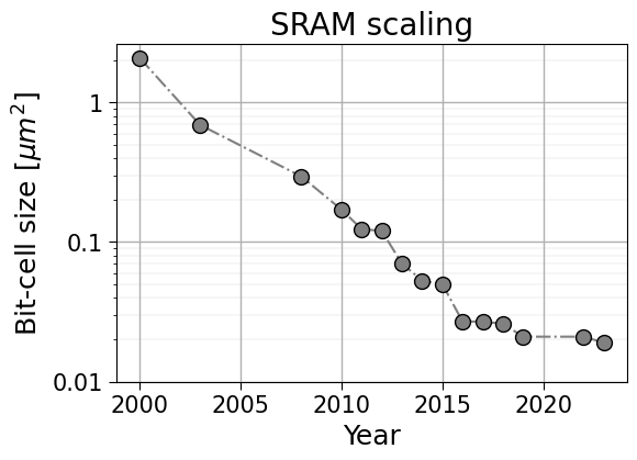
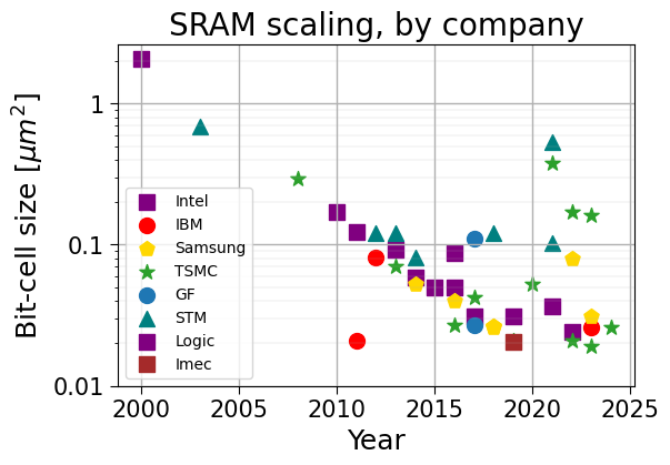
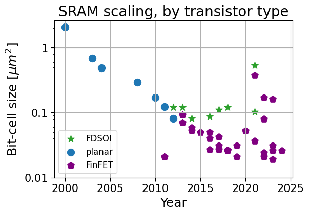
This data, again, is reported in the shared spreadsheet and from it we can learn three main messages:
- 1: SRAM bit-cell size has steadily decreased through the years, but it appears to have slowed down lately.
- 2: planar CMOS technology hit a wall at the beginning of the 2010s, when FinFET technology took over and continued the scaling trend.
- 3: only three companies are currently participating in the race of SRAM scaling (TSMC, Samsung, Intel).
As technology nodes become more advanced, the investments required to participate in the silicon scaling race grow exponentially. This is why the leading edge of SRAM scaling is carried out by essentially only one company nowadays, TSMC. Samsung follows closely, and Intel seems to be lagging a little behind.
Will SRAM scaling continue?
It seems like SRAM scaling is becoming harder and harder, and even TSMC flinched when launching its 3nm node, with the N3B specification offering only a 5% improvement over the N5 (5nm) node [1]. However, the semiconductor industry still has some tricks up its sleeves, and it is ready to play them all to ensure the continuation of SRAM scaling.
- Nanosheet transistors: the next generation of transistors promises higher integration density, guaranteeing the continuation of SRAM scaling.
- Backside power rails: an option mainly researched by Intel.
- Forksheet transistor: a development of Gate-All-Around transistors enabling greater transistor density.
- Complementary 3D stacked logics: a potentially disruptive technology whereby p- and n-mos transistors can be stacked on top of each other, offering clear scaling advantages even compared to ultimate nanosheet transistors.
Alternative emerging memory technology
Embedded Non-Volatile Memory (eNVM)
As advanced technology nodes become ever more expensive and technically challenging, very few companies can afford to continue CMOS development. This leads researchers to explore novel memory devices that operate by exploiting different physical phenomena. This class of emerging memories has been discussed a lot, so how does it compare with SRAM? We’ll now focus on emerging non-volatile memory (eNVM), which includes RRAM, MRAM, PCM, and FeRAM. (The latter is not mature enough to be compared in the following plots.)
Scroll through the 2 figures!
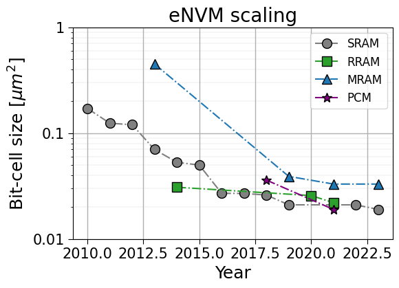
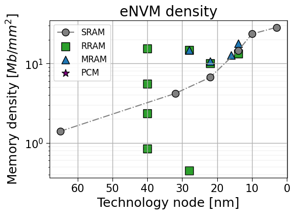
This data, once more, is reported in the shared spreadsheet:
- 1: in terms of bit-cell size, eNVM is competitive with SRAM, especially RRAM and PCM.
- 2: however, memory array density highlights that eNVM is, for now, reserved for larger technology nodes (typically 40nm or 28nm, topping at 14nm), and thus eNVM is currently less memory-dense.
For now we have mainly looked at size and density, but there is more to memory. The next figure gives an idea of the figures of merit of different memory technologies, comparing SRAM (in gray) to eNVM. Note that this figure is obtained by considering the general performance of the different memory classes, taking inspiration from Table 1 in [8].
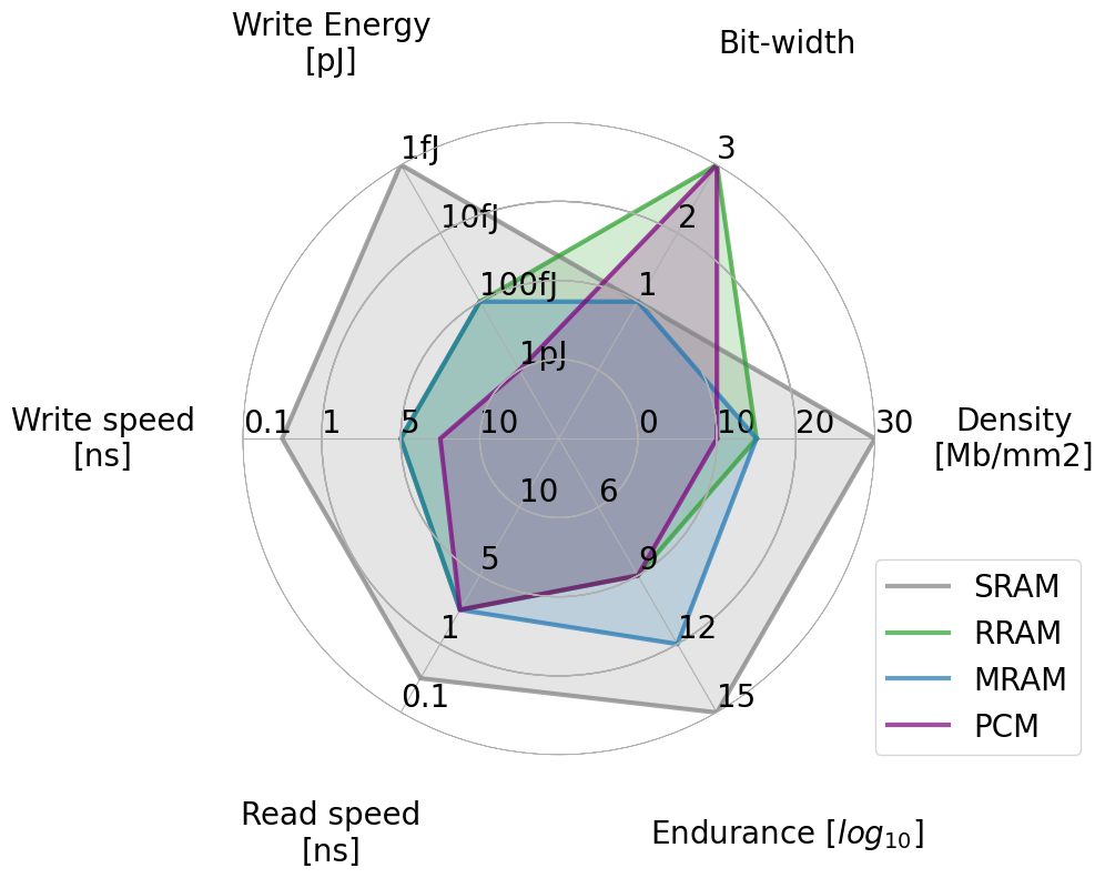
What do we learn? SRAM and eNVM are apples and oranges. They do not belong to the same class of memory devices, which are famously clustered in the memory pyramid (refer to Figure 2 in [8]). In particular, the core differences are:
- SRAM is fast! eNVM is slower to read and even slower to write.
- SRAM has extremely high endurance (number of read/write cycles before failure). MRAM also features high endurance, but RRAM and PCM are very limited in this sense.
- Despite SRAM being the densest so far, RRAM and PCM feature multi-bit per cell. The density gap might close in the future!
The future of memory technology
(What follows is my personal opinion)
It is hard to predict what the future of memory technology will look like. My opinion is that until transistor scaling will be physically possible and economically viable, industry will keep developing in that direction, bringing benefits to SRAM scaling. Concerning memory applications, it’s hard to see SRAM dethroned as L1 and L2 cache memory, where sheer speed is mandatory. There is no other device currently capable to deliver similar read and write speed.
However, transistor scaling will likely hit a point of diminishing returns at some point. Are the alternative memory devices ready to take over when this happens? Again, it depends on the applications.
- eNVM is already in the market, as embedded memory in commercial micro-controllers [9].
- As L3 or L4 cache memory, MRAM might evolve into a serious candidate, especially when its non-volatility can be exploited in low stand-by power contexts.
Compute-In-Memory
The most intriguing domain of application for eNVM is certainly Compute-in-Memory (CIM). While SRAM-based CIM is definitely high-performing, breaking the 1000 Tops/W mark per macro, eNVM-based CIM is also competitive [10]. eNVM features two important characteristics that are still not fully exploited in CIM, especially in low-power applications. While SRAM is the speed king and maximally efficient only at peak frequency, eNVM does not consume any static power (in theory!), and it is thus energy-efficient even at low frequency, a typical use case for edge applications. Also, RRAM and PCM store multiple bits per cell (typically 3 bits): this aspect is rarely exploited as it makes peripheral circuit design more complex (you need to design a compact ADC), but it might give an edge to eNVM in terms of CIM memory density.
Scaling in the third dimension
But there is an important prospect to account for: 3D memory integration [11]. Nowadays, 3D integration is reserved for Flash memory, achieving more than 100 levels in the Back-End-of-Line and thus record-breaking memory density [12]. SRAM is very likely not scalable to 3D, as crystalline silicon cannot be deposited in the BEOL to form the six transistors required by SRAM. In contrast, eNVM is already BEOL-compatible. So can it scale to 3D? Yes, but it will be complicated. Some early research showed BEOL integration of RRAM and a carbon-nanotube selector [13], potentially scalable to multiple 3D layers. This paves the way toward ultra-high on-chip memory density.
Thanks for reading! Please do not hesitate to provide feedback; you can find my contacts on the landing page of my website (provide links!). Also check out the Emerging Intelligent Substrates Lab (EIS), directed by Melika Payvand. It is a cool environment where novel memristive-based architectures and neuromorphic algorithms are co-designed, leading to creative and competitive neuromorphic solutions.
Visit the EIS Lab GitHub.
References
[1] David Schorr “IEDM 2022: Did We Just Witness The Death Of SRAM?” WikiChip Fuse (2022)
[2] Wong, H-S. Philip, et al. “Metal–oxide RRAM.” Proceedings of the IEEE 100.6 (2012): 1951–1970.
[3] Ielmini, Daniele, et al. “Physical interpretation, modeling and impact on phase change memory (PCM) reliability of resistance drift due to chalcogenide structural relaxation.” 2007 IEEE International Electron Devices Meeting. IEEE, 2007.
[4] Na, Taehui, Seung H. Kang, and Seong-Ook Jung. “STT-MRAM sensing: a review.” IEEE Transactions on Circuits and Systems II: Express Briefs 68.1 (2020): 12–18.
[5] Mikolajick, Thomas, et al. “FeRAM technology for high density applications.” Microelectronics Reliability 41.7 (2001): 947–950.
[6] Liu, Shuhan, et al. “Hybrid 2T nMOS/pMOS Gain Cell Memory with Indium-tin-oxide and Carbon Nanotube MOSFETs for Counteracting Capacitive Coupling.” IEEE Electron Device Letters (2023).
[7] Fredeman, Gregory, et al. “A 14 nm 1.1 Mb embedded DRAM macro with 1 ns access.” IEEE Journal of Solid-State Circuits 51.1 (2015): 230-239.
[7] Dalgaty, Thomas, et al. “In situ learning using intrinsic memristor variability via Markov chain Monte Carlo sampling.” Nature Electronics 4.2 (2021): 151–161.
[8] Mannocci, P., et al. “In-memory computing with emerging memory devices: Status and outlook.” APL Machine Learning 1.1 (2023).
[9] STMicroelectronics, announcing an 18nm FD-SOI platform with ePCM.
[10] Shanbhag, Naresh R., and Saion K. Roy. “Comprehending in-memory computing trends via proper benchmarking.” 2022 IEEE Custom Integrated Circuits Conference (CICC). IEEE, 2022.
[11] Vianello, Elisa, and Melika Payvand. “Scaling neuromorphic systems with 3D technologies.” Nature Electronics 7.6 (2024): 419-421.
[12] Kim, Bvunarvul, et al. “28.2 A High-Performance 1Tb 3b/Cell 3D-NAND Flash with a 194MB/s Write Throughput on over 300 Layers” 2023 IEEE International Solid-State Circuits Conference (ISSCC). IEEE, 2023.
[13] Srimani, Tathagata, et al. “Foundry monolithic 3D BEOL transistor+ memory stack: Iso-performance and Iso-footprint BEOL carbon nanotube FET+ RRAM vs. FEOL silicon FET+ RRAM.” 2023 IEEE Symposium on VLSI Technology and Circuits (VLSI Technology and Circuits). IEEE, 2023.